ZHCSIK6D November 2017 – June 2024 ADS8166 , ADS8167 , ADS8168
PRODUCTION DATA
- 1
- 1 特性
- 2 应用
- 3 说明
- 4 Pin Configuration and Functions
- 5 Specifications
- 6 Detailed Description
-
7 Register Maps
- 7.1
Interface and Hardware Configuration Registers
- 7.1.1 REG_ACCESS Register (address = 00h) [reset = 00h]
- 7.1.2 PD_CNTL Register (address = 04h) [reset = 00h]
- 7.1.3 SDI_CNTL Register (address = 008h) [reset = 00h]
- 7.1.4 SDO_CNTL1 Register (address = 0Ch) [reset = 00h]
- 7.1.5 SDO_CNTL2 Register (address = 0Dh) [reset = 00h]
- 7.1.6 SDO_CNTL3 Register (address = 0Eh) [reset = 00h]
- 7.1.7 SDO_CNTL4 Register (address = 0Fh) [reset = 00h]
- 7.1.8 DATA_CNTL Register (address = 10h) [reset = 00h]
- 7.1.9 PARITY_CNTL Register (address = 11h) [reset = 00h]
- 7.2 Device Calibration Registers
- 7.3 Analog Input Configuration Registers
- 7.4
Channel Sequence Configuration Registers Map
- 7.4.1 DEVICE_CFG Register (address = 1Ch) [reset = 00h]
- 7.4.2 CHANNEL_ID Register (address = 1Dh) [reset = 00h]
- 7.4.3 SEQ_START Register (address = 1Eh) [reset = 00h]
- 7.4.4 SEQ_ABORT Register (address = 1Fh) [reset = 00h]
- 7.4.5 ON_THE_FLY_CFG Register (address = 2Ah) [reset = 00h]
- 7.4.6 AUTO_SEQ_CFG1 Register (address = 80h) [reset = 00h]
- 7.4.7 AUTO_SEQ_CFG2 Register (address = 82h) [reset = 00h]
- 7.4.8
Custom Channel Sequencing Mode Registers
- 7.4.8.1 CCS_START_INDEX Register (address = 88h) [reset = 00h]
- 7.4.8.2 CCS_END_INDEX Register (address = 89h) [reset = 00h]
- 7.4.8.3 CCS_SEQ_LOOP Register (address = 8Ah) [reset = 00h]
- 7.4.8.4 CCS_CHID_INDEX_m Registers (address = 8C, 8E, 90, 92, 94, 96, 98, 9A, 9C, 9E, A0, A2, A4, A6, A8, and AAh) [reset = 00h]
- 7.4.8.5 REPEAT_INDEX_m Registers (address = 8D, 8F, 91, 93, 95, 97, 99, 9B, 9D, 9F, A1, A3, A5, A7, A9, and ABh) [reset = 00h]
- 7.5
Digital Window Comparator Configuration Registers Map
- 7.5.1 ALERT_CFG Register (address = 2Eh) [reset = 00h]
- 7.5.2 HI_TRIG_AINx[15:0] Register (address = 4Dh to 30h) [reset = 0000h]
- 7.5.3 LO_TRIG_AINx[15:0] Register (address = 71h to 54h) [reset = 0000h]
- 7.5.4 HYSTERESIS_AINx[7:0] Register (address = 4Fh to 33h) [reset = 00h]
- 7.5.5 ALERT_LO_STATUS Register (address = 78h) [reset = 00h]
- 7.5.6 ALERT_HI_STATUS Register (address = 79h) [reset = 00h]
- 7.5.7 ALERT_STATUS Register (address = 7Ah) [reset = 00h]
- 7.5.8 CURR_ALERT_LO_STATUS Register (address = 7Ch) [reset = 00h]
- 7.5.9 CURR_ALERT_HI_STATUS Register (address = 7Dh) [reset = 00h]
- 7.5.10 CURR_ALERT_STATUS Register (address = 7Eh) [reset = 00h]
- 7.1
Interface and Hardware Configuration Registers
- 8 Application and Implementation
- 9 Device and Documentation Support
- 10Revision History
- 11Mechanical, Packaging, and Orderable Information
6.4.1.3 Auto Sequence Mode
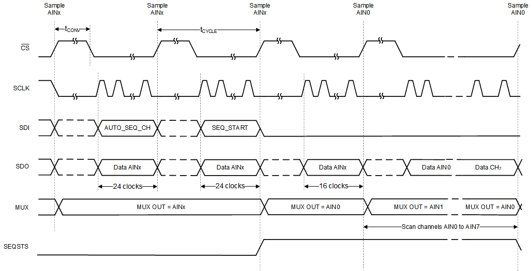
In auto sequence mode, the internal channel sequencer selectively scans channels from AIN0 through AIN7 in ascending order. To select auto sequence mode, configure SEQ_MODE to 10b in the DEVICE_CFG register using a 3-byte register access. Enable one or more channels among AIN[7:0] by configuring the AUTO_SEQ_CFG1 register. By default all analog input channels are enabled. After enabling the desired channels, start the sequence by setting SEQ_START to 1b. The ADC auto-increments through the enabled channels after every CS rising edge. Configure SEQSTS_CFG bit to 1b in SDO_CNTL4 register to indicate sequence status on SDO-1/SEQSTS pin. When SEQ_START is set to 1b, the SDO-1/SEQSTS pin is at logic 1 as shown in Figure 6-14 until the last channel conversion frame is complete. After the last enabled channel conversion is complete, channel AIN0 is selected and SDO-1/SEQSTS is in a high-impedance state.
 Figure 6-14 Starting a Sequence in Auto
Sequence Mode
Figure 6-14 Starting a Sequence in Auto
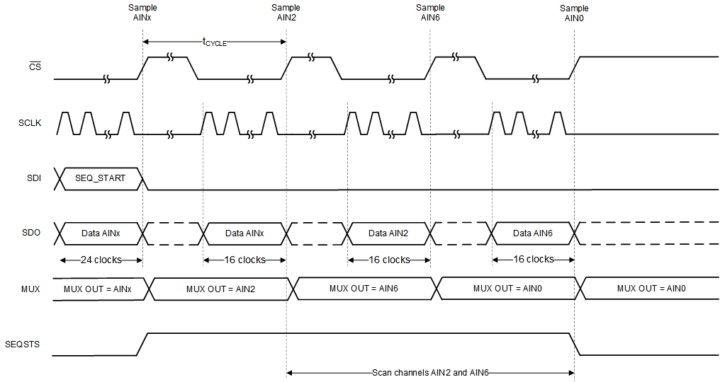
Sequence ModeAs an example, Figure 6-15 depicts a timing diagram for when the device is scanning AIN2 and AIN6 in auto sequence mode. When AIN6 is converted, SDO-1/SEQSTS is Hi-Z and AIN0 is selected as the active channel. At the end of sequence, if more conversion frames are launched the device returns valid data corresponding to AIN0.
To use the device in auto sequence mode follow these steps:
- Set the SEQ_MODE[1:0] bits in the DEVICE_CFG register to 10b.
- Configure the AUTO_SEQ_CFG1 register. In Figure 6-15, AUTO_SEQ_CFG1 = 0x44.
- Set the SEQ_START bits in the SEQ_START register to 1b to start executing the sequence.
- Optionally, configure SEQSTS_CFG bit to 1b in SDO_CNTL4 register to indicate sequence status on SDO-1/SEQSTS pin.
 Figure 6-15 Example: Scanning Channels 2
and 6 in Auto Sequence Mode
Figure 6-15 Example: Scanning Channels 2
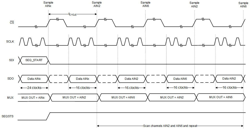
and 6 in Auto Sequence ModeTo repeat a channel sequence indefinitely, set the AUTO_REPEAT bit in the AUTO_SEQ_CFG2 register to 1b. Figure 6-16 shows that when the AUTO_REPEAT bit is enabled, the MUX scans through the channels enabled in the AUTO_SEQ_CFG1 register and repeats the sequence after the last channel data are converted.
 Figure 6-16 Example: Scanning Channels 2
and 6 in Auto Sequence Mode With AUTO_REPEAT = 1
Figure 6-16 Example: Scanning Channels 2
and 6 in Auto Sequence Mode With AUTO_REPEAT = 1Figure 6-16 provides a timing diagram for when the device is scanning AIN2 and AIN6 in auto sequence mode with AUTO_REPEAT = 1b. When AIN6 is converted, AIN2 is selected as the active channel and the device continues scanning through the enabled channels again.
To use the device in auto sequence with the repeat mode enabled follow these steps:
- Set the SEQ_MODE[1:0] bits in the DEVICE_CFG register to 10b.
- Configure the AUTO_SEQ_CFG1 register. In Figure 6-15, AUTO_SEQ_CFG1 = 0x44.
- Set AUTO_REPEAT to 1b.
- Set the SEQ_START bit in the SEQ_START register to 1b to start executing the sequence.
- Optionally, configure SEQSTS_CFG bit to 1b in SDO_CNTL4 register to indicate sequence status on SDO-1/SEQSTS pin.
To terminate an ongoing channel sequence set the SEQ_ABORT bit in the SEQ_ABORT register 1. When SEQ_ABORT is set, the auto sequence stops and AIN0 is selected as the active input channel.