SNCS104D April 2005 – December 2014 LMH6570
PRODUCTION DATA.
7 Application and Implementation
NOTE
Information in the following applications sections is not part of the TI component specification, and TI does not warrant its accuracy or completeness. TI’s customers are responsible for determining suitability of components for their purposes. Customers should validate and test their design implementation to confirm system functionality.
7.1 Application Information
The LMH6570 is a high-speed 2:1 analog multiplexer, optimized for very high speed and low distortion. With selectable gain and excellent AC performance, the LMH6570 is ideally suited for switching high resolution, presentation grade video signals. The LMH6570 has no internal ground reference. Single or split supply configurations are both possible, however, all logic functions are referenced to the mid supply point. The LMH6570 features very high speed channel switching and disable times. When disabled the LMH6570 output is high impedance making MUX expansion possible by combining multiple devices. See Multiplexer Expansion. The LMH6570 SEL defaults to logic low (IN0 active). The default state for the SD pin is also logic low (device enabled). Both pins can be left floating if the default state is desired.
7.2 Typical Application
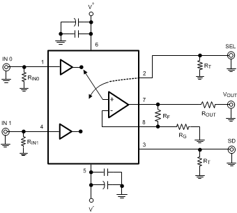 Figure 25. Typical Application
7.2.1 Video Performance
The LMH6570 has been designed to provide excellent performance with production quality video signals in a wide variety of formats such as HDTV and High Resolution VGA. Best performance will be obtained with back-terminated loads. The back termination reduces reflections from the transmission line and effectively masks transmission line and other parasitic capacitances from the amplifier output stage. Figure 25 shows a typical configuration for driving a 75-Ω cable. The output buffer is configured for a gain of 2, so using back terminated loads will give a net gain of 1.
7.2.2 Feedback Resistor Selection
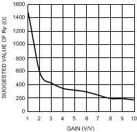 Figure 26. Suggested RF vs. Gain
The LMH6570 has a current feedback output buffer with gain determined by external feedback (RF) and gain set (RG) resistors. With current feedback amplifiers, the closed loop frequency response is a function of RF. For a gain of 2 V/V, the recommended value of RF is 576 Ω. For other gains, see Figure 26. Generally, lowering RF from the recommended value will peak the frequency response and extend the bandwidth while increasing the value of RF will cause the frequency response to roll off faster. Reducing the value of RF too far below the recommended value will cause overshoot, ringing and, eventually, oscillation.
Since all applications are slightly different, it is worth some experimentation to find the optimal RF for a given circuit. For more information see Current Feedback Loop Gain Analysis and Performance Enhancement, Application Note OA-13 (SNOA366), which describes the relationship between RF and closed-loop frequency response for current feedback operational amplifiers. The impedance looking into pin 8 is approximately 20 Ω. This allows for good bandwidth at gains up to 10 V/V. When used with gains over 10 V/V, the LMH6570 will exhibit a “gain bandwidth product” similar to a typical voltage feedback amplifier. For gains of over 10 V/V consider selecting a high performance video amplifier like the LMH6720 to provide additional gain.
7.2.3 Multiplexer Expansion
It is possible to use multiple LMH6570 devices to expand the number of inputs that can be selected for output. Figure 27 shows a 4:1 MUX using two LMH6570 devices.
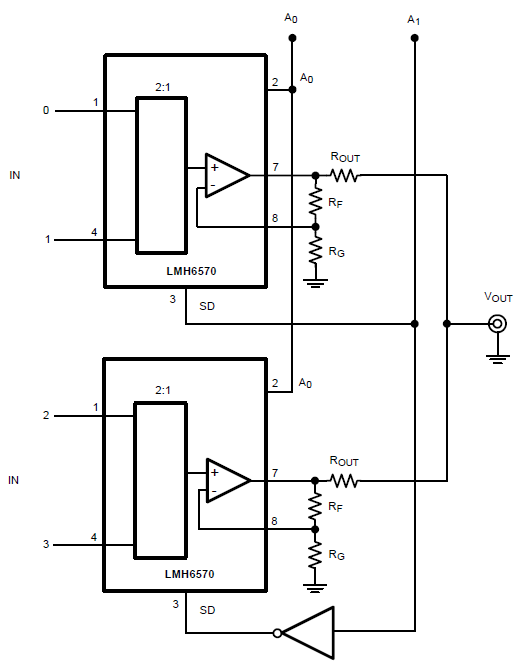 Figure 27. 4:1 MUX Using Two LMH6570 Devices
In such an application, the output settling may be longer than the LMH6570 switching specifications (~20 ns), while switching between two separate LMH6570 devices. The switching time limiting factor occurs when one LMH6570 is turned off and another one is turned on, using the SD (shutdown) pin. The output settling time consists of the time needed for the first LMH6570 to enter high impedance state plus the time required for the second LMH6570 output to dissipate left-over output charge of the first device (limited by the output current capability of the second device) and the time needed to settle to the final voltage value.
While Figure 27 MUX expansion benefits from more isolation, originating from the parasitic loading of the un-selected channels on the selected channel, afforded by individual ROUT on each multiplexer output, this configuration does not produce the fastest transition between individual LMH6570 devices. For fastest transition between LMH6570 devices, the configuration of Figure 28 can be used where the LMH6570 output pins are all shorted together.
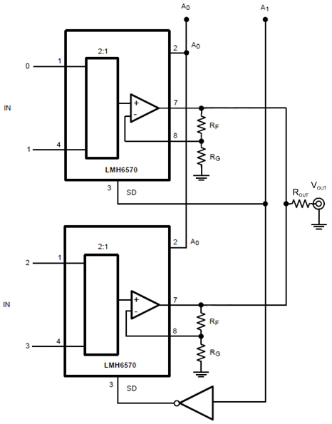 Figure 28. Alternate 4:1 MUX Expansion Schematic (for Faster SD Switching)
Figure 29 shows typical transition waveforms and shows that SD pin switching settles in less than 145 ns.
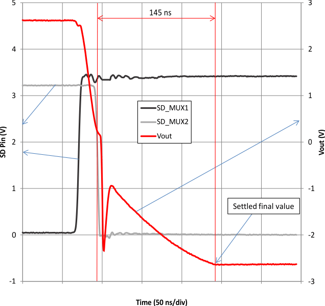 Figure 29. SD pin Switching Waveform and Output Settling
If it is important in the end application to make sure that no two inputs are presented to the output at the same time, an optional delay block can be added, to drive the SHUTDOWN pin of each device. Figure 30 shows one possible approach to this delay circuit. The delay circuit shown will delay H to L transitions of SHUTDOWN (R1 and C1 decay) but will not delay its L to H transition. R2 should be kept small compared to R1 in order to not reduce the SHUTDOWN voltage and to produce little or no delay to SHUTDOWN.
 Figure 30. Delay Circuit Implementation
With the SHUTDOWN pin putting the output stage into a high impedance state, several LMH6570 devices can be tied together to form a larger input MUX. However, there is a loading effect on the active output caused by the unselected devices. The circuit in Figure 31 shows how to compensate for this effect. For the 8:1 MUX function shown in Figure 31, the gain error would be about 0.7% or −0.06dB. In the circuit in Figure 31, resistor ratios have been adjusted to compensate for this gain error. By adjusting the gain of each multiplexer circuit the error can be reduced to the tolerance of the resistors used (1% in this example).
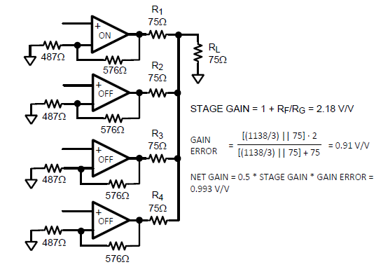 Figure 31. Multiplexer Gain Compensation
NOTE
Disabling of the LMH6570 using the EN pin is not recommended for use when doing multiplexer expansion. While disabled, If the voltage between the selected input and the chip output exceeds approximately 2 V the device will begin to enter a soft breakdown state. This will show up as reduced input to output isolation. The signal on the non-inverting input of the output driver amplifier will leak through to the inverting input, and then to the output through the feedback resistor. The worst case is a gain of 1 configuration where the non-inverting input follows the active input buffer and (through the feedback resistor) the inverting input follows the voltage driving the output stage. The solution for this is to use shutdown mode for multiplexer expansion.
7.2.4 Other Applications
The LMH6570 could support a dual antenna receiver with two physically separate antennas. Monitoring the signal strength of the active antenna and switching to the other antenna when a fade is detected is a simple way to achieve spacial diversity. This method gives about a 3 dB boost in average signal strength and is the least expensive method for combining signals.
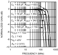
7.2.5 Driving Capacitive Loads
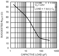
Capacitive output loading applications will benefit from the use of a series output resistor ROUT. Figure 32 shows the use of a series output resistor, ROUT, to stabilize the amplifier output under capacitive loading. Capacitive loads of 5 to 120 pF are the most critical, causing ringing, frequency response peaking and possible oscillation. Figure 33 gives a recommended value for selecting a series output resistor for mitigating capacitive loads. The values suggested in the charts are selected for 0.5 dB or less of peaking in the frequency response. This gives a good compromise between settling time and bandwidth. For applications where maximum frequency response is needed and some peaking is tolerable, the value of ROUT can be reduced slightly from the recommended values.
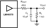 Figure 32. Decoupling Capacitive Loads
7.2.6 ESD Protection
The LMH6570 is protected against electrostatic discharge (ESD) on all pins. The LMH6570 will survive 2000-V Human Body model and 200-V Machine model events. Under normal operation the ESD diodes have no effect on circuit performance. However, there are occasions when the ESD diodes will be evident. If the LMH6570 is driven by a large signal while the device is powered down, the ESD diodes will conduct. The current that flows through the ESD diodes will either exit the chip through the supply pins or will flow through the device. Therefore, it is possible to power up a chip with a large signal applied to the input pins. Using the shutdown mode is one way to conserve power and still prevent unexpected operation.